")
")
")
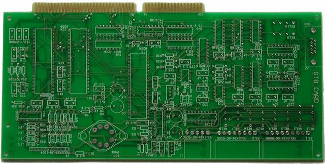
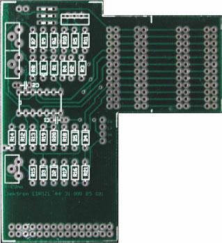
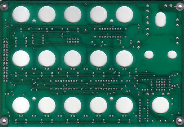
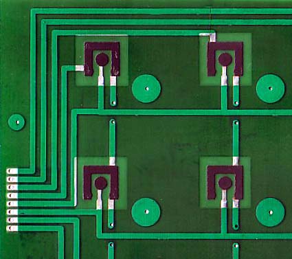
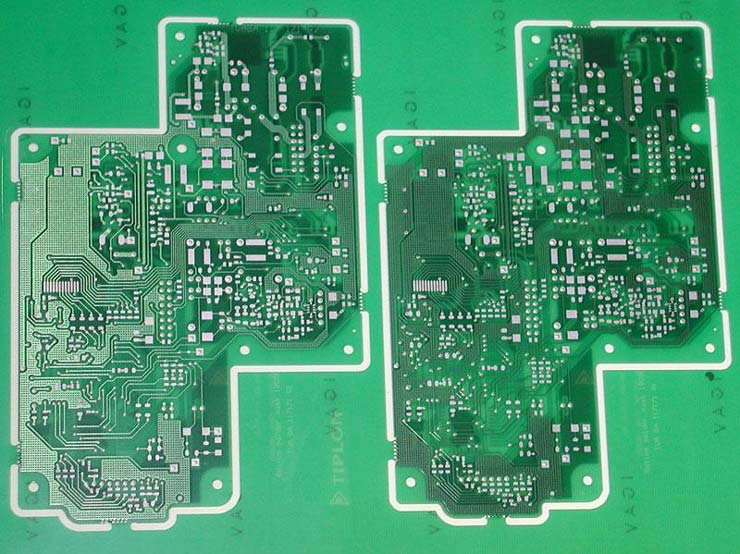
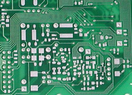
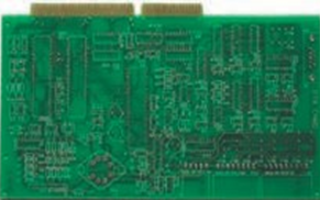
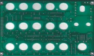
According to the documentation and requirements of the customer, we produce electronic printed boards that enable safe and high quality connection of electrical components in devices and machines.
DOCUMENTATION: It is necessary to submit a GERBER file in the RS 274 - X version with the inclusion list and DRILL file in EXCELLON 2 or jpeg, cdr, pdf, gif, tif, dxf, dwg, hpgl or a quality draft on paper.
QUALITY CONTROL: 100% optical control, 200X digital microscope, 200 mA current current, sample microcontroller, certificates for all materials, final product conformity control report
CERTIFICATES: ISO 9001 quality standard - ISO 14001 environmental protection standard - in the certification process
Production standard: for product quality acceptability, we use the IPC-600H standard
By purchasing our products you get quality assurance - customer satisfaction is our primary concern.
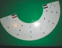
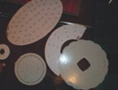
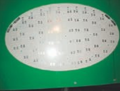
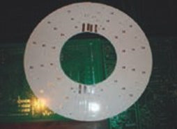
Copper laminates: FR2, CEM , FR4, TEFLON , ROGER , ALUMINUM, POLYAMID..
We offer various types of copper laminates with different temperature stability characteristics Tg 135-260 ° C, dielectric permittivity Er, thermal conductivity W / mK ... detailed technical data TDS and MSDS sheets are provided on request.
Insulation thickness: 0.15-0.20-0.35-0.50-0.65-0.80-1.00-1.20-1.40-1.60-1.80-2.00 ... 4.0 mm and on request other thickness. Tolerance of insulation thickness is <+ 0.10 mm.
Copper foil thickness: 18, 35, 70, 105, 140, 210 μm and on request other thickness.
The basic thickness of the copper foil is applied min. 20 μm of galvanic copper. The copper thickness in the holes is min. 20 μm
Solder resistant varnish:
-gloss or mat - suitable for automatic and manual soldering, temperature resistant in soldering devices,
-options: black mat, white, red, blue, transparent and other shades, dielectric strength 93 kV/mm, bullet class: UL 94 V-0. The thickness of the lacquer after thermal treatment is min. 15 μm
-tin-lead alloy (Sn63Pb37) - (Sn63Pb37) - low temperature standard alloy, melting temperature 183 ° C, solderability for min. 1 year, tin (SnCu0,7Ni) RoHS alloy, melting temperature at 227 ° C, solderability for min. 1 year.
-tin (Sn) RoHS - good for SMD components and contacts, solderable at 230 °C - solderability min. 6 months
-solder lacquer - transparent organic lacquer, solderable at 215 °C - solderability min. 6 months
-nickel-gold (Ni / Au) - solder coating , high oxidation resistance, for PC slots and contacts, solderability min. 2 years.
-carbon varnish - the graphite conductive layer is used for contact surface for the keys, resistors, connectors, sensors, etc.
-removable thermoresistant lacquer- for temporary protection during automatic soldering.
-marking & service print: epoxide colors: white, yellow, black and other shades... resistant to temperature in soldering machines.
OTHER TECHNICAL DATA: Width of lines and spacing: optimally 0.25 mm (10 mil), minimum 0.15 mm (6 mil) Standard panel dimensions: <600 x 300 mm, special requirements < 900 x 600 mm
standard dimensions 160x100 mm and 200x160 mm, with raster 2.54 mm and 5.08 mm.